International Journal of Theoretical and Applied Nanotechnology (IJTAN)
ISSN: 1929-1248

Volume 9 - Year 2021 - Pages 08-13
DOI: 10.11159/ijtan.2021.002
Electronic Properties of SiC Nanotubes: Quantum Simulation
Qiyin Luo1, Mitsuhiro Matsumoto1
1Graduate School of Engineering, Kyoto University
Kyoto-daigaku-Katsura, Kyoto 615-8540, Japan
luoqiyin2012@gmail.com; matsumoto@kues.kyoto-u.ac.jp
Abstract - We performed a series of quantum simulations for the geometrics, electronic structures and electron transport of various types of silicon carbide nanotubes (SiCNT's). The 1:1 SiCNT's generally show more stable semi-conducting behaviour than carbon nanotubes (CNT's). The SiCNT's exhibit better electronic properties than their bulk crystal and expanded sheets. Next, we found out that these tubes' band gap increases with increasing the tube diameter. Armchair SiCNT's have narrower band gap than zigzag ones, whereas the zigzag SiCNT's possess a direct band gap. Finally, we investigated how adsorbed atoms affect the electronic structure. Three cases of hydrogen atoms adsorbed on different sites were examined, showing different semiconducting properties. These results indicate the potential application of SiCNT's in fields of electronic devices.
Keywords: Silicon carbide nanotubes, Quantum simulation, Electronic structures, Band gap, Electron transport.
© Copyright 2021 Authors - This is an Open Access article published under the Creative Commons Attribution License terms. Unrestricted use, distribution, and reproduction in any medium are permitted, provided the original work is properly cited.
Date Received: 2020-12-20
Date Accepted: 2020-12-22
Date Published: 2021-02-17
1. Introduction
Since the discovery of carbon nanotubes (CNT's) by Iijima [1] much interest has been focused on quasi-one-dimensional nanomaterials because of their potential use in nanotechnology and nanoscale engineering.
As for their application in semiconductor fields, the electronic properties depend on their chirality, to be more specific, the chiral vector (n,m) [2-4], which makes it difficult and troublesome to synthesize precise types of CNT's. Only when (n-m)=3k±1, where k is an integer, the CNT's show semiconducting properties. Thus, finding other materials possessing more stable semiconducting properties to reduce the uncertainty in manufacturing is highly desirable. There has been much expectation that other materials, such as silicon-based ones, with similar nano-scale structures have more stable semiconducting properties.
Among the various types of semiconducting materials, silicon carbide possesses unique physical and electronic properties, and its application to electronic devices has been pursued. These one-dimensional materials have shown unusual properties such as extremely high strength, large flexibility, fracture toughness and the inverse Hall-Petch effect leading to the wide range of applications [5-6]. Since the success in synthesis of boron nitride nanotubes [7-9], various types of low-dimensional materials of non-carbon or partial carbon compounds have been explored. Two-dimensional silicon (silicene) was found to be unstable [10], for example. However, C-C and Si-C bonds are known to be more stable than the Si-Si bond, which can be utilized to stabilize Si nanotubes [11]. Furthermore, the formation of the SiCNT's has been investigated in Ref. [12], by a disproportionation reaction of silicon oxide with carbon nanotubes in a tube furnace. Thus, it provides a new possibility to fabricate this kind of semiconducting materials.
We focus on silicon carbide nanotubes (SiCNT's), which may have electronic properties much different from their bulk materials. In this paper, we systematically explore the electronic properties of various SiCNT's using quantum simulations.
2. Methods
We adopted the density functional tight binding (DFTB) model for the quantum simulation to investigate the structure, electronic properties, and electron transport behaviours of SiCNT's. The DFTB+ package [13] was utilized.
A self-consistent charge (SCC) calculation was carried out with the relative tolerance of charge fluctuations 10-7. The periodic boundary condition is set along the tube axis (𝑧), while the vacuum space of 30Å is assumed for the radial directions to evaluate the properties of a single tube. The supercell contains 16 layers of atoms along the tube axis for both armchair and zigzag types. The number of k points is chosen to be (1×1×4). We adopted the matsci-3-0 parameter set [14] for the Slater-Koster parameters.
For each SiCNT, we performed a molecular dynamics (MD) calculation with temperature control; after constructing an initial atomic configuration, we gradually raised the temperature to look into the mechanical stability. In this paper, results at 300K are mainly reported. The average length of Si-C bonds was about 1.80Å, in agreement with Ref. [15].
3. Results and Discussion
Various types of SiCNT's with different diameters and chiralities (zigzag-type or armchair-type) were prepared, where Si and C atoms are placed alternatively without any adjacent atoms of the same element. After equilibrating the system at 300 K, electronic properties were investigated.
3.1. Density of States Analysis
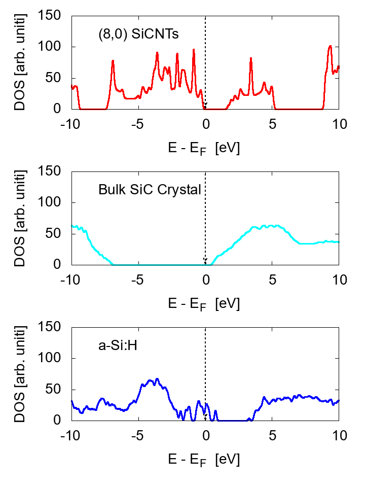
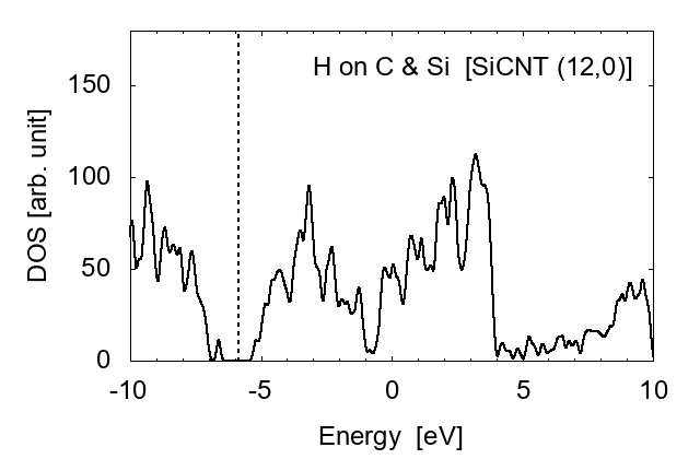
Examples of the density of states (DOS) are shown in Fig. 1 for zigzag-type (12,0) and armchair type (7,7) SiCNT's; both types are semiconductor with a narrow band gap. The energy gap is approximately 1.80 eV for zigzag (12,0) and 1.51 eV for armchair (7,7). To elucidate the feature of SiCNT's, we compare the DOS in Fig. 2 among the (8,0) SiCNT, bulk SiC crystal, and the hydrogenated amorphous silicon sample [16], which indicates that the SiCNT has much narrower band gap than the bulk crystal, suggesting a good semi-conducting property (i.e., high conductivity) of SiCNT's.
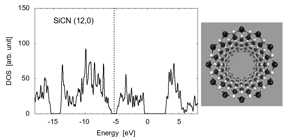
(a) Zigzag type, (12, 0)
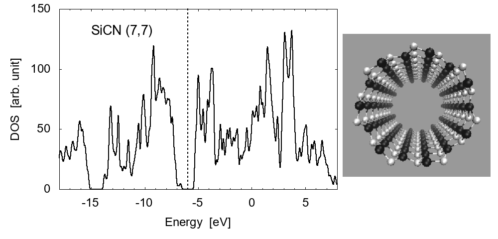
(b) Armchair type, (7, 7)
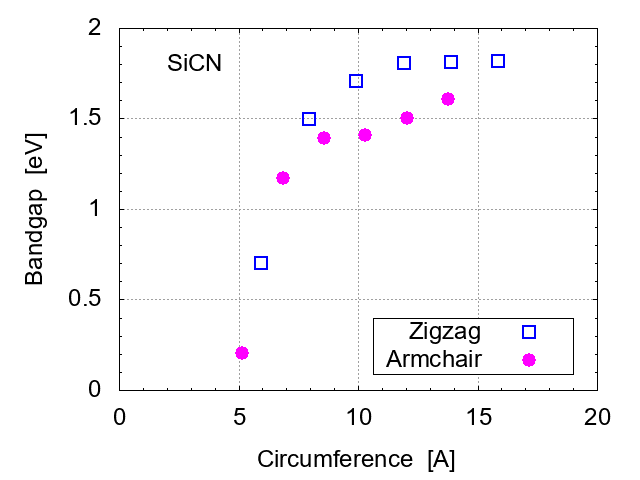
3.2. Size Dependence of Band Gap
For further investigation, size (circumference of SiCNT) dependence of the band gap is evaluated, as shown in Fig. 3, for zigzag types and armchair ones. The band gap becomes wider for thicker tubes. Armchair types have slightly narrower gaps than zigzag ones. It is interesting to note that all of the SiCNT's are semiconductors, in contrast to CNT's, in which armchair types are metallic.
3.3. SiCNTs vs. SiC sheet
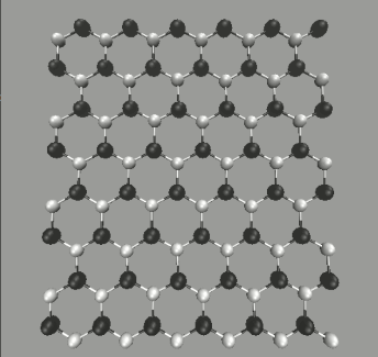
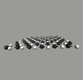
To make further comparison, we cut and unfolded the zigzag-type SiCNT's into SiC sheets. An example is shown in Fig. 4 (top), where the unfolded sheet spread on x-y plane. The size is assumed to be infinite using the periodic boundary conditions. The snapshot indicates that the configuration of SiC sheet is similar to graphene but with a slight wiggling. The average bond length after equilibration is about 1.80Å, while the bond angle 118.1∘, in agreement with an experimental value [5].
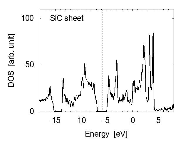
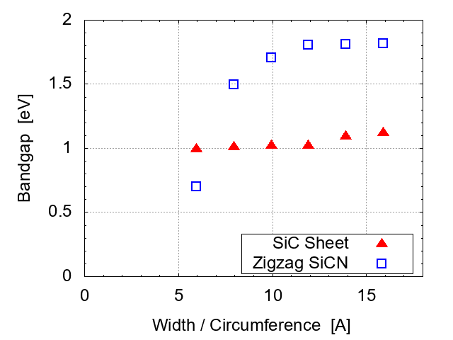
The energy gap of this SiC sheet is about 1.93 eV, showing relatively poor conductivity than SiCNT's. The band gap of SiC sheet has a slight dependence on the size (i.e., the width along x direction, corresponding to the circumference of the corresponding SiCNT). Comparison with the zigzag-type SiCNT's is made in Fig. 5. SiC sheets have better conductivity than zigzag SiCNT's when the circumference of SiCNT's is larger than ~7Å.
3.4. Electron Transport
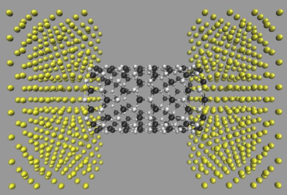
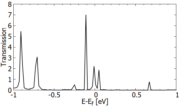
The electronic transport properties were evaluated based on the non-equilibrium Green's function method [13]; an example is shown in Fig. 6, where both ends of a (12,0) SiCNT are contacted with metallic electrodes (aluminum fcc crystal) and the transmission coefficient is evaluated. There exists a significant transmission around the Fermi level ϵF, suggesting the importance of the detailed electronic states around ϵF for the application of SiCNT's in electronic devices.
Zigzag type: direct bandgap
Armchair type: indirect bandgap
3.5. Types of Band Gap
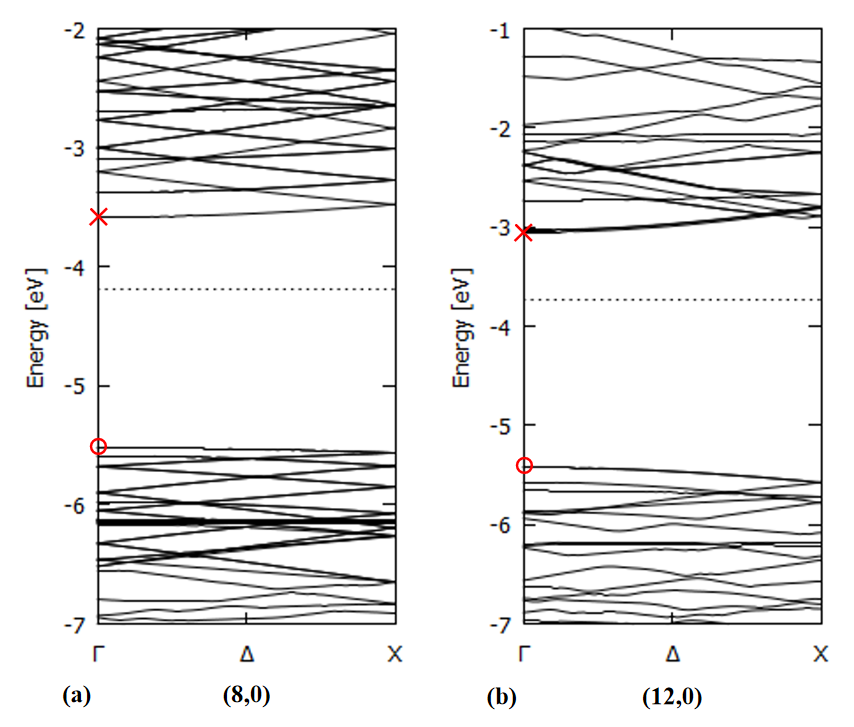
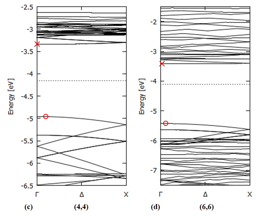
Examples of the band structure along the tube axis are shown in Fig. 7 for several SiCNT's. It's apparent that the zigzag types have a direct band gap while the armchair types have only an indirect one. No direct band gaps are reported for bulk SiC crystal [36 B], suggesting the possible application of SiCNT's for light-emitting devices.
3.6. Adsorbed Hydrogen Atom
Finally, we investigated the effect of hydrogen atoms adsorbed on the side wall of SiCNT's. Three cases were examined: H adsorbed on a carbon atom, H on a silicon atom, and two H's on both C and Si. Examples for (12, 0) SiCNT are shown in Fig. 8.
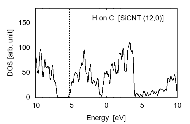
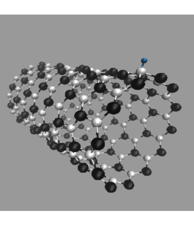
H adsorbed on C
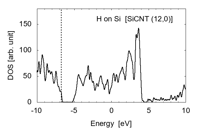
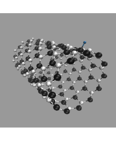
H adsorbed on Si
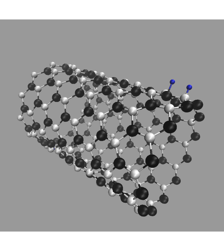
Two H atoms adsorbed on C and Si
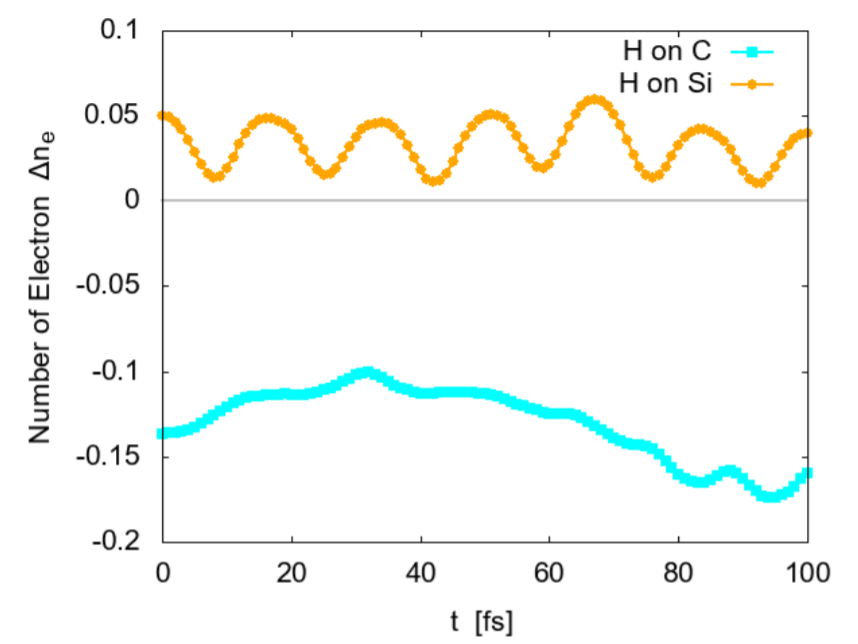
It is shown that the adsorbed hydrogen atoms largely shift the Fermi level ϵF. When an H is adsorbed on a C atom, ϵF shifts from the center of the bandgap to the lowest unoccupied conduction band (LUCB), displaying the characters of n-type semiconductors. To the opposite, with an H on a silicon atom, ϵF is close to the highest occupied valence band (HOVB), suggesting p-type semiconductor. As shown in Fig. 9, electrons tend to transfer from H to C, and from Si to H. The difference in electronegativity seems to explain this behavior. The Pauling's value [17] is 2.20 for H, 2.55 for C, and 1.90 for Si; thus H works as a donner on C, and an accepter on Si. When hydrogen atoms are adsorbed on both C and Si, these effects are cancelled each other, and the DOS returns to that of intrinsic semiconductors.
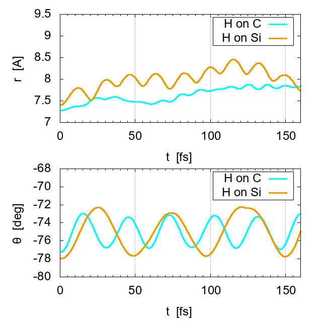
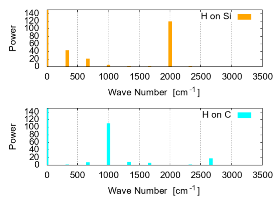
To examine the adsorption strength, the change of spatial position of the adsorbed H is plotted in Fig. 10. The plot is done in the cylindrical coordinates, where r is the radial distance from the nanotube axis, roughly corresponding to the bond-stretching motion, while θ is the angular position around the nanotube; the plot for the coordinate z is not shown since the positional change along the axis is small and slow. Apparently the amplitude of radial oscillation for H-Si is larger than that for H-C, suggesting that adsorption on C is more stable, probably due to larger charge transfer, as shown in Fig. 9. On the other hand, the H-Si stretching has higher frequency than that of the H-C one, as shown in Fig. 11.
4. Conclusion
A series of quantum simulations based on the DFTB model were performed to investigate the electronic properties of various types of silicon carbide nanotubes (SiCNT's). SiCNT's generally possess a much narrower band gap than their bulk crystal, depending on their thickness (diameter). The band gap of armchair types is still narrower than that of zigzag types. When the circumference of SiCNT's is larger than ~7Å, SiC sheets show better conductivity than zigzag SiCNT's. Direct band gap exists in the zigzag type SiCNT's while the armchair types have indirect one. The electron transport calculations suggest that the electronic states around the Fermi level have major contribution to the total current. These findings are useful for designing various types of SiCNT's devices, such as light emitting diodes and molecular transistors. Hydrogen-decorated SiCNT's show different types of semiconductors depending on the adsorbed position.
References
[1] S.Iijima,“Helical microtubules of graphitic carbon,” Nature (London), 354, 2148 (1991). View Article
[2] J. W. Mintmire, B. I. Dunlap, and C. T. White, “Are fullerene tubules metallic,” Phys. Rev. Lett. 68, 631 (1992). View Article
[3] N. Hamada, S. I. Sawada, and A. Oshiyama, “New one-dimensional conductors: Graphitic microtubules,” Phys. Rev. Lett. 68,1579 (1992). View Article
[4] R. Saito, M. Fujita, G. Dresselhaus, and M. S Dresselhaus, “Electronic structure of chiral graphene tubules,” Appl. Phys. Lett. 60, 2204 (1992). View Article
[5] Properties of Silicon Carbide, edited by G. L. Harris (INSPEC, Institution of Electrical Engineers, London, 1995).
[6] J. Prakash, R venugopalan, and B.M. Tripathi, “Chemistry of one dimensional silicon carbide materials: Principle, production, application and future prospects,” Progress in Solid State Chemistry, 43, 98-122 (2015). View Article
[7] N.G. Chopra, R.J. Luyken, K. Cherry, V.H. Crespi, M.L. Cohen, S.G. Louie, and A. Zettl, “Boron nitride nanotubes,” Science, 269, 966-967 (1995). View Article
[8] A. Loiseau, F. Willaime, N. Demoncy, G. Hug, and H. Pascard, “Boron nitride nanotubes with reduced numbers of layers synthesized by arc discharge,” Phys. Rev. Lett., 76, 4737-4740 (1996). View Article
[9] D. Goldberg, Y. Bando, W. Han, K. Kurashima, and T. Sato, “Single-walled B-doped carbon, B/N-doped carbon, and BN nanotubes synthesized from SWCNTs through a substitution reaction,” Chem. Phys. Lett. 308, 337-342 (1999). View Article
[10] F.S. Khan and J.Q. Broughton,“Relaxation of icosahedral-cage silicon clusters via tight-binding molecular dynamics,” Phys. Rev. B, 43, 11754-11761 (1991). View Article
[11] M. Menon, E. Richter, A. Mavrandonakis, G. Froudakis, and A.N. Andriotis, “Structure and stability of SiC nanotubes,” Phys. Rev. B, 69, 115322 (2004). View Article
[12] X. Sun, C. Li, W. Wong, N. Wong, C. Lee, S. Lee, and B. Teo, “Formation of silicon carbide nanotubes and nanowires via reaction of silicon (from disproportionation of silicon monoxide) with carbon nanotubes,” J. Am. Chem. Soc, 124, 14464–14471 (2002). View Article
[13] http://www.dftbplus.org/about-dftb/ View Article
[14] https://dftb.org/parameters View Article
[15] C. Tabtimsai, V. Ruangpornvisuti, S. Tontapha and B. Wanno, “A DFT investigation on group 8B transition metal-doped silicon carbide nanotubes for hydrogen storage application,” Applied Surface Science, 439, 494-505(2018). View Article
[16] H. Li and M. Matsumoto, “Structure and electronic properties of a-Si:H investigated with quantum simulation,” Proc. TANN'20 (2020) no. 136.
[17] L. Pauling, “The nature of chemical bond,” J. Am. Chem. Soc., 54, 3570-3582 (1932). View Article