International Journal of Theoretical and Applied Nanotechnology (IJTAN)
ISSN: 1929-1248

Volume 8 - Year 2020 - Pages 13-20
DOI: 10.11159/ijtan.2020.003
Nanostructured Chalcogenide Thin Films Synthesized by Chemical Methods for Photovoltaic Applications
Yuri Vorobiev1, Francisco Willars-Rodriguez1, Fernando Chimal-Moreno1, Rafael RamírezBon1, C.E. Perez-Garcia2, Pavel Vorobiev3
1 CINVESTAV-Querétaro, Libramiento Norponiente #2000, Querétaro 76230, Qro, México
vorobiev@cinvestav.mx; fwillars@cinvestav.mx; fernando.chimal@cinvestav.mx; rrbon@cinvestav.mx
2Universidad Autónoma de Querétaro, Cerro de las Campanas S.N., CP.76010, Querétaro, QRO, México,
claudia.pergar@gmail.com
3CIMAV-Monterrey, Alianza Norte 202, PIIT, Apodaca 66628, N. L., México,
pavel.vorobiev@cimav.edu.mx
Abstract - - The chalcogenide semiconductors, like CdS, CdSe, CdTe, PbS, PbSe are of great interest for photovoltaic applications, in particular, due to the possibility to be part of multi-layered (tandem) photovoltaic converters. These materials are not expensive and can be produced by economic and ecologically friendly techniques like CBD (Chemical Bath Deposition) and its recent versions (SILAR - Successive Ionic Layer Adsorption and Reaction, and LACBD – Light Assisted Chemical Bath Deposition). It is known that nano--porosity is an essential feature of these techniques. In this paper we study its effects upon the band gap values; the corresponding band gap variations can be used for optimizing the device efficiency. The porosity was modeled by close-packed ball system. In general, we conclude that the quantum confinement effects caused by nano-structuration of semiconductor thin films for photovoltaic converters improve the converter’s parameters.
Keywords: Chalcogenide semiconductors, CBD, SILAR, LACBD, porosity, nano structuration, quantum effects.
© Copyright 2020 Authors - This is an Open Access article published under the Creative Commons Attribution License terms. Unrestricted use, distribution, and reproduction in any medium are permitted, provided the original work is properly cited.
Date Received: 2020-11-07
Date Accepted: 2020-11-10
Date Published: 2020-12-14
1. Introduction
Today a continuous increase of the utilization of renewable sources of energy worldwide is observed, due to the permanent problems with fossil fuels and the ecological problems; this situation is not alien to Mexico. In particular, because of that the interest towards photovoltaic materials increases: semiconductors like gallium arsenide GaAs with 1.43 eV direct band gap and cadmium telluride CdTe having 1.5 eV direct band gap are ones of the most promising as light absorbers in solar cells according to Shockley and Quiesser estimations [1]. CdSe has the band gap of 1.7 eV and can be either n-type or p-type, so it is also very promising in these applications. The common CdS/CdTe solar cell is a simple heterojunction structure [2] containing a p-doped CdTe light absorbing layer (can be substituted by p-CdSe film) matched with an n-doped CdS film, which acts also as a window layer. Another useful application of these or similar structure is photovoltaic light detector (sensor); for these devices Schottky diode structure might be preferable.
The other chalcogenide semiconductors (like PbS, PbSe, PbTe) are also very interesting for photovoltaic applications: in some of them the multi exciton generation was observed [3], besides these can be part of efficient multi-layered light-to-electricity converters (an example of CdS/PbS solar cell made by CBD technique we presented in [4]). These materials are not expensive contrary to III-V compounds frequently used in photovoltaic devices, the techniques of their production are economic and ecologically friendly like ammonium free CBD (Chemical Bath Deposition) and its recently developed versions (SILAR - Successive Ionic Layer Adsorption and Reaction, and LACBD – Light Assisted Chemical Bath Deposition). Materials produced by these methods are usually nano porous; this porosity causes the corresponding quantum confinement that affects the band gap value. The corresponding band gap variation can be regulated by experimental conditions; for illustration, in PbS we observed the band gap variation between 0.4 and 0.8 eV [4, 5]. Thus, within the family of materials discussed (CdS, CdSe and PbS) we have a set of band gaps of approximately 2.4, 1.7 and 0.8 eV sufficient to cover the whole solar spectrum in corresponding multi-union solar cell.
This paper presents a description of preparation and investigation of semiconductor thin films mentioned above, and the discussion of the effects of quantum confinement caused by porosity on the materials optical properties.
2. Materials and Methods
To improve the electrical properties of CdS films, we doped them with Sn, Al and Eu with the idea that these atoms have more valence electrons than Cd and thus must act as donors. Besides, Eu atoms having incomplete internal electron shell can also possess luminescent and magnetic properties that might add new options of possible material applications. The thin films of cadmium sulfide were made using the technique of ammonia free chemical bath deposition CBD assisted by ultraviolet light illumination (LACBD). As substrates we used ITO-on-glass layers, commercial glass slides and p-type silicon wafers (these in attempt to create photo diode structure). The deposition was made in a total bath volume of 50 ml adding sequentially the following reagents: 15 ml of 0.05 M cadmium chloride (CdCl2 J.T.Baker ® 99.3% purity), 15 ml of 0.5 M sodium citrate (C6H5O7Na3, J.T.Baker ® 99.1% purity), 2.5 ml of 0.5 M potassium hydroxide (KOH, Sigma-Aldrich ® 89.13% purity), 2.5 ml of pH 10 buffer solution (J.T.Baker ® 100% purity), 3.75 ml of 0.5 M thiourea (CS(NH2)2 J.T.Baker ® 99.6% purity). For Sn doping, various concentration of 5 mM of stannous chloride were added (SnCl2∙2H2O, J.T.Baker ® 99.3% purity); for Al and Eu doping, the reagents used were aluminum chloride (AlCl3∙6H2O, J.T.Baker ® 99.1% purity) and europium nitrate (Eu(NO3)3∙5H2O, Sigma Aldrich ® 98.1% purity). The solution was diluted with deionized water to have a total volume of 50 ml.
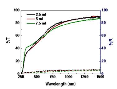
CdSe was prepared in a similar way using Na2SeSO3 instead of thiuorea that was a source of sulfur in CdS preparation, the complete procedure is described in [6]. The amount of sodium citrate was varied between 2.5 and 7.5 ml in solution, for studying its effect upon the films adhesion. The best results correspond to 7.5 ml. The deposition of PbS film by chemical bath was presented in [4].
PbS was prepared by SILAR method, using 0.5M lead acetate solution complexed with 0.1M triethanolamine (TEA) and 0.2M thioacetamide as cationic and anionic precursors respectively. The optimized absorption and reaction time for cationic and anionic precursors was found at 60 and 30 s correspondingly. The number of cycles was varied between 15 and 60. The thickness of all films obtained varied between 100 and 500 nm.
X-ray diffraction (XRD) of samples was measured by a multipurpose X-ray diffraction system (XRD, Rigaku Co., UltiIV, Japan) with Cu (Kα1/α2=1.5406Å/1.5444Å) source. The diffractograms were recorded at room temperature between angles 20° to 80° with a scan rate of 1°/min and step size 0.005°. Optical properties were studied in a Spectrometer (SCI Co., FilmTek 3000, CA., USA) in the wavelength range of 240 nm to 950 nm; the information obtained from the measurement was used to calculate the bandgap for each sample. The work function was measured with the Kelvin probe system (SKP KP Technology, SKP5050), work function resolution 5-10 meV (50 µm tip), the SKP instrument is equipped with a tungsten-halogen light source to measure surface photovoltage as a function of intensity. For studying the morphological properties, a Field Emission Scanning Electron Microscope was used (JEOL Ltd, JSM-7610F, Japan). The film composition was determined using energy dispersive X-ray analysis (Electron Dispersion Spectroscopy with SEM, Philips Co., XL30 ESEM, Netherland).
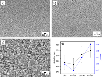
The measurement’s errors are defined, first of all, by the corresponding device calibration. In case of XRD data, the calibration with monocrystalline silicon was performed giving the experimental error in finding the crystal lattice constants in 0.001 Å that enables determination of the lattice distortion caused by substitution of the lattice atoms by another atoms different in atomic size. In optical measurements, the SCI FilmTek 3000 instrument was calibrated with 2 standards (Si wafer and Si/SiO2 wafer) and the errors in measurements of transmission and reflection were less than 5%. The accuracy in determination of samples band gap by a standard extrapolation technique we estimate as 0.01 eV. In estimation of the grain size from SEM images, the error is determined by actual dispersion of sizes: here 40 measurements were made for each sample, and then the average and standard deviation were calculated (shown in corresponding figure).
3. Results and Discussion
3.1 Morphology and Structure
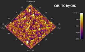
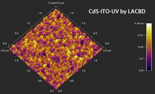
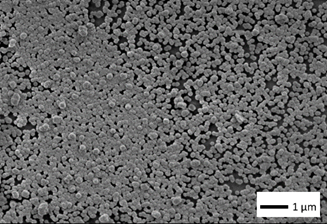
The results of the morphologic study on CdS:M thin films (M being the doping metal atom) are shown in Figure 1, here a typical morphology for a CdS films obtained from CBD technique was observed [7]. The superficial morphology exhibits a homogenous composition, absence of pin-holes, lack of cracks through the film; further the films present spherically shaped grains. It is observed that the grain size increases as a function of the dopant added to the CBD solution. The structural properties analyzed with AFM are presented in Figure 2. The observed AFM data is compared between films of CdS-ITO (normal CBD) and CdS-ITO-UV (LACBD). It can be observed that “light assisted CBD” film has higher roughness. SEM image of CdSe film is presented in Figure 3. Here, same as in CdS case and PbS, close-packed spherical grains are observed, with pores among them.
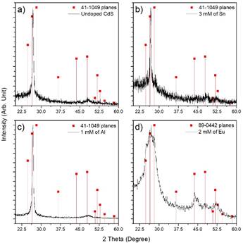
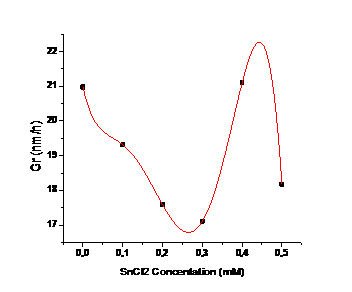
The crystallographic properties of CdS thin films doped with different metals were evaluated via X-ray diffraction, the patterns are shown in Figure 4, where two diffraction peaks are observed at ~26.5° and ~48° related with the (002) and (103) crystalline planes for the hexagonal phase of CdS (this behavior is observed in aluminum- and tin-doped cadmium sulfide films and undoped CdS), this information is confirmed from ICDD card No. 41-1049. Eu-doped cadmium sulfide diffractogram exhibit several peaks at ∽26.1°, 36.1°, 44.2°, 48.4° and 52.2° corresponding to the planes (002), (102), (110), (103) and (112) for the hexagonal phase of CdS or Greenockite (PDF No. 41-1049). Obtained from diffractograms crystallite size was around 20 nm for all films except Eu-doped ones. (See Figure 5 for CdS:Sn samples with different doping).
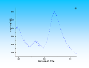
Photoluminescence (PL) results measurements (Figure 6) reveal the blue shift of electronic transitions from the band gap energy suggesting that these near boundary layers can be treated as quantum wells with the corresponding quantum confinement effects. Here we see the bands at 400, 530 and 680 nm corresponding to photons 3.1, 2.34 and 1.83 eV. The last two are related to the defects, and according to [7] can be ascribed to S interstitials (2.34 eV) and ICdVCd complexes (1.83 eV). But, the first band exceeds the bulk band gap value by approximately 0.6 eV and definitely indicates the quantum confinement effect.
The doping of CdS films has profound effect on their electrical properties enhancing the conductivity, which allowed us to prepare Schottky diodes on their basis that can be used as efficient photosensors; these results will be published separately. Here we concentrate on the discussion of quantum effects caused by nano structuration of the materials obtained.
3.2 Optical properties
The results of optical study of CdSe films (transmission and reflection spectra) are given in Figure 7. It shows general transmission of around 80 % in near infrared and absorption in visible region, indicating that the material obtained can serve as good absorbed layer in solar cell having corresponding thickness.
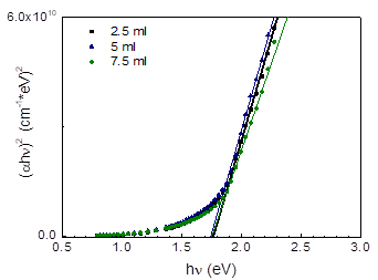
In Figure 8 the diagram normally used for determination of the band gap for CdSe is presented, for samples with the different amount of sodium citrate during preparation. It is seen that the average band gap value is 1.755 eV, a little higher than the bulk value known from the literature (1.74 eV), the sodium nitrate amount having practically no effect on the band gap.
The average band gap value for CdS:Sn films found from optical data (see [8]) was equal to 2.47 eV that is somewhat higher than the bulk value (2.42 eV), this point will be discussed below. The data for CdS:Al is quite similar.
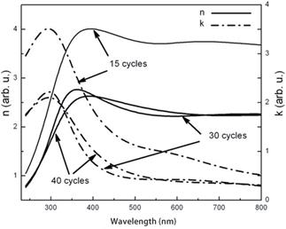
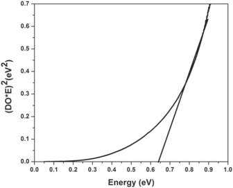
In Figures 9 and 10 optical properties of SILAR-made PbS films are presented. It should be noted that the material´s refractive index is lower than the bulk value that definitely indicates the porosity (the variations with number of cycles show that porosity changes non-monotously with an increase of sample thickness). And another indication of porosity effects is the band gap value (0.64 eV, Figure 10) essentially greater than the bulk value of 0.41 eV.
3.3 Discussion of quantum effects
In the materials and structures studied, two types of quantum confinement effects are observed: one connected with near-boundary quantum wells (blue shift of CdS photoluminescence spectrum), and another resulting from the material porosity (band gap blue shift found in CdS, CdSe and PbS). The first effect was analyzed in previous publication [5]; here we discuss the second one.
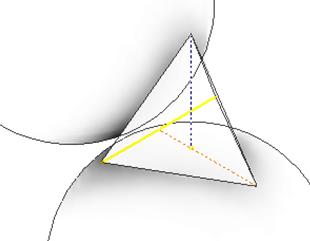
Our approach is based on the Even Mirror Boundary Conditions (EMBC) in solution of the Schrödinger equation (see [9-11]). Earlier we have described the porosity-stimulated effects upon the band gap of CBD-made materials [12] treating the pores as “Quantum Anti-Dots” (voids surrounded by semiconductor material, with mirror-reflecting walls allowing again application of our original Mirror Boundary Conditions). On the basis of XRD and SEM data mentioned, we assume that our samples have the closely packed structure of ball-shaped crystallites. In this case a pore is formed by four adjacent balls (see Figure 11) and its shape can be modeled by a tetrahedral pyramid formed by planes touching the balls in centers of facets. We describe electron’s interaction with the ball surface (for an electron approaching a pore from within a crystallite) equalizing its Ψ-function in a near-surface point with the one of its image in a spherical wall-mirror, similar to the case analyzed in [11] for a spherical quantum dot; at small distances, a spherical surface can be approximated by a plane.
In
dense packing of equal spheres (theory in [13]) the spheres occupy 74% of the
total volume. For every sphere
there is one gap (void or pore) surrounded by six spheres (octahedral one) and
two gaps surrounded by four spheres (tetrahedral). The distances to the centers
of these gaps from the centers of the surrounding spheres is ![]() for the
tetrahedral, and
for the
tetrahedral, and ![]() for the
octahedral, when the sphere radius is taken as 1. We restrict ourselves with
analysis of tetrahedral pores (being smaller than octahedral ones, they cause
greater quantum confinement effect).
for the
octahedral, when the sphere radius is taken as 1. We restrict ourselves with
analysis of tetrahedral pores (being smaller than octahedral ones, they cause
greater quantum confinement effect).
Thus, total voids have 26% of the volume; so, their summary pore volume for one sphere is 26/74 = 0.35% of a volume of a sphere. If we neglect the octahedral void, then each tetrahedral one has 0.175% of a sphere volume. Then we approximate a tetrahedral pore as tetrahedron – a pyramid formed by 4 equilateral triangles – it gives a possibility to find a relation between tetrahedron side a and diameter D (or radius R) of a sphere. The volume of tetrahedron

and the volume of sphere

from the equality Vt = 0.175 Vsp we find that a = 0.92 D = 1.84 R.
It is clear that this approximation gives exaggerated size of actual tetrahedral pore; we made another estimation by calculation of the volume of tetrahedron that touches four spheres in a tetrahedral pore. This approach gives a = 1.1 R. The average of these two approximations gives a = 1.47 R.
Our calculations of the energy spectra of pyramidal quantum dots based on EMBC approach (see argumentation in [14]) give for tetrahedral pyramid the expression

m being
electron effective mass, ![]() - the Planck
constant, and n - quantum number.
- the Planck
constant, and n - quantum number.
In the following discussion, we assume that typical pores in CBD materials are smaller than the Bohr radius αB for an exciton (α/2 < αB) which is important for the case of exciton formation under the illumination [15]. In all semiconductors studied (CdS, CdSe, PbS) the value of αB exceeds 20 nm according to the expression below

with exciton reduced mass

Here, me,h is the electron/hole effective mass, є is the dielectric constant of the material, and єo is a permittivity constant. Following the argumentation given in [9, 15, 16], we see that for the blue shift estimation one can directly apply the expressions for energy spectra because the separation between the quantum levels proportional to ħ2/ma2 is large compared to the Coulomb interaction between the carriers which is proportional to e2/єєoα. Therefore, Coulomb interaction can be neglected, and the energy levels could be found from quantum confinement effect alone. Accordingly, we shall calculate the emission/absorption photon energy for transitions corresponding to the exciton ground state, which is given in Eq. 3 by n = 1. Thus, we will assume that the fundamental absorption edge corresponds to generation of an exciton with ground state energy:
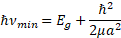
Eg being the semiconductor bulk band gap.
The bulk Eg value in CdS at room temperature is 2.42 eV. Our optical data give band gap value of 2.47 eV for Sn-doped thin films prepared. To explain the edge shift hνmin - Eg of 0.05 eV observed (exciton reduced mass in CdS [17] 0.134 m0), one obtains from Eq. 6 the tetrahedral pore size a = 10 nm. Taking the relation above between the value of a and the “ball radius” R as a/R = 1.42, we obtain the ball radius R equal to 14 nm that quite agrees with the crystallite size cited above. Thus, we see that our assumption about the internal porosity as a cause of band gap blue shift agrees with the experimental data.
4. Conclusion
Two kinds of nano-structuration were observed and investigated in chalcogenide films prepared for application in photovoltaic light-to-electricity converters, both causing the quantum confinement effects and the corresponding blue shift of electronic transitions: one due to variation of films composition near their boundaries, and another due to porosity inherent to all materials produced by Chemical Bath Deposition (thus we conclude that used in our work SILAR and Light Assisted Chemical Bath Deposition – LACBD also possess this quality). Theoretical description of pore-induced blue shift based on our original Mirror Boundary Conditions in “particle in a box” quantum problem agrees with experimental data. All effects examined can be used for monitoring of materials and structures parameters and are profitable for photovoltaic converters.
Acknowledgements
F. Willars-Rodriguez and F. Chimal-Moreno wish to thank CONACYT for their scholarship. We are thankful to Prof. Paul Horley for fruitful discussion of quantum effects, and want to acknowledge the technical assistance of: Luis Gerardo Silva Vidaurri, C.A. Avila Herrera, J.E. Urbina Alvárez, A. Jiménez Nieto.
References
[1] W. Shockley, H. J. Queisser, ¨Detailed Balance Limit of Efficiency of pn Junction Solar Cells¨, Journal of Applied Physics, vol. 32, pp. 510-519, 1961. View Article
[2] R.G. Dhere, et al., "Development of substrate structure CdTe photovoltaic devices with performance exceeding 10%", Proc. 38th IEEE PVSC pp. 3208-3211, 2012 View Article
[3] R.J. Ellingson, M.C. Beard, J.C. Johnson, P. Yu, O.I. Micic, A.J. Nozik, A. Shabaev, A.L. Efros, ¨Highly efficient multiple exciton generation in colloidal PbSe and PbS quantum dots¨, Nano Letters, vol. 5, pp. 865–871, 2995. View Article
[4] J. Hernandez Borja, Y. V. Vorobiev, R. Ramirez Bon, “Thin film solar cells of CdS/PbS chemically deposited by an ammonia-free process” Solar Energy Materials & Solar Cells, vol. 95, pp. 1882-1888, 2011. View Article
[5] C.E. Perez-Garcia, S. Meraz-Dávila, G. ArreolaJardón, F. de Moure-Flores, R. Ramírez-Bon and Y.V. Vorobiev, “Characterization of PbS films deposited by successive ionic layer adsorption and reaction (SILAR) for CdS/PbS solar cells application” Materials Research Express, 7 (2020) 015530. View Article
[6] H. E. Esparza-Ponce, J. Hernández-Borja, A. Reyes-Rojas, M. Cervantes-Sánchez, “Growth technology, X-ray and optical properties of CdSe thin films” Materials Chemistry and Physics, vol. 113, pp. 824–828, 2009. View Article
[7] D. Wu, Yang Jiang, Yugang Zhang, Yongqiang Yu, Zhifeng Zhu, Xinzheng Lan, Fangze Li, Chunyan Wu, Li Wang and Linbao Luo, “Self-powered and fast-speed photodetectors based on CdS:Ga nanoribbon/Au Schottky diodes” Journal of Materials Chemistry, vol. 22, pp. 23272–23276, 2012. View Article
[8] Y. V. Vorobiev, I. R. Chávez-Urbiola, S. A. Pérez-García, P. Vorobiev, “Quantum confinement effects in a GLASS/ITO/CdS/CdTe superstrate structure designed for solar energy conversion”, Proceedings of ISER International Conference, Paris, France, 11th-12th October 2016, ISBN: 978-93-86083-34-0.
[9] Y. V. Vorobiev, P. M. Gorley, V. R. Vieira, P. P. Horley, J. González-Hernández, T. V. Torchynska, A. Diaz Cano, “Effect of Boundary Conditions on the Energy Spectra of Semiconductor Quantum Dots Calculated in the Effective Mass Approximation”, Physica E, vol. 42, pp 2264-2267, 2010. View Article
[10] Y. V. Vorobiev, T. V. Torchynska, P. P. Horley, “Effect of Aspect Ratio on Energy of Optical Transitions in a Pyramid-Shaped Quantum Dot”, Physica E, vol. 51, pp 42-47, 2013. View Article
[11] Y. V. Vorobiev, P. M Gorley, V. R. Vieira and P. P. Horley, “Electronic States in Nanostructures and Quantum Dots”, Proceedings of International Conference on Innovative Technologies (Bahadurgarh, India, 2009), pp. 19-29.
[12] J. H. Conway, N. J. Sloane, A. B. Eiichi, in Sphere packings, lattices, and groups. Springer. 1999, Section 6.3. View Article
[13] F. J. Willars-Rodríguez, I. R. Chávez-Urbiola, M. A. Hernández-Landaverde, P. Vorobiev, R. Ramirez-Bon, Y. V. Vorobiev, “Effects of tin-doping on cadmium sulfide (CdS:Sn) thin-films grown by light-assisted chemical bath deposition process for solar photovoltaic cell”, Thin Solid Films, vol. 653 (2018), pp. 341-349. View Article
[14] F. J. Willars-Rodríguez, I. R. Chávez-Urbiola, M. A. Hernández-Landaverde, P. Vorobiev, R. Ramirez-Bon, Y. V. Vorobiev, “Effects of tin-doping on cadmium sulfide (CdS:Sn) thin-films grown by light-assisted chemical bath deposition process for solar photovoltaic cell”, Thin Solid Films, vol. 653 (2018), pp. 341-349. View Article
[15] S. V. Gaponenko, Optical Properties of Semiconductor Nanocrystals. Cambridge: Cambridge University Press; 1998. View Article
[16] Y.V. Vorobiev, F.J. Willars-Rodriguez, F.Chimal-Moreno, R. Ramírez-Bon, P. Vorobiev, Proceedings of the 5th World Congress on Recent Advances in Nanotechnology (RAN'20) Lisbon, Portugal, Virtual Congress– October 2020, Paper No. ICNNFC 153, 2020.
[17] J. Singh, Physics of Semiconductors and Their Heterostructures. New York: McGraw-Hill, 1993.