International Journal of Theoretical and Applied Nanotechnology (IJTAN)
ISSN: 1929-1248

Volume 2, Year 2014 - Pages 9-17
DOI: 10.11159/ijtan.2014.002
Prospective Application of A3B3C62 Type Semiconductors for Developing Nano-size Electronic Devices
Arif Pashaev1, Arif Badalov1, Rauf Sardarly2, Oktay Samedov2, Nurana Alieva2, Rayiha Agayeva2, Aygun Orujova2, Arzu Sardarli3
1Azerbaijan National Academy of Aviation, Baku, Bina, AZ1045, Azerbaijan Republic
mail@naa.edu.az; m.t14@mail.ru
2Institute of Radiation Problems, National Academy of Sciences of Azerbaijan, Baku, B.Vaxabzade 9, AZ1143, Azerbaijan Republic
sardarli@yahoo.com; o.samedov@rambler.ru; nur.elizade@rambler.ru; aqayevaraya@rambler.ru; aygun.orucova@list.ru
3First Nations University of Canada, 1301 Central Ave, Prince Albert, SK, S6V 4W1, Canada
asardarli@fnuniv.ca
Abstract - In this paper we present the most recent results of our studies on TlInTe2 and TlInSe2 crystals (continuing our earlier studies on TaGaTe2), and analyze the nano-size application perspectives of A3B3C62 semiconductors. It has been shown that A3B3C62 semiconductors are prospective materials for developing the nano-size devices such as varistors, solid electrolytic accumulators and supercapacitors. The analysis is based on our experimental studies, which include the temperature dependence of the electrical conductivity, THz spectra, and permittivity. It has been shown that the electrical conductivity parameters of A3B3C62 type semiconductors can be affected by γ-irradiation, and the effect depends on the dose of irradiation. The possibility of restructuring of electrical conductivity mechanism in these semiconductors makes them attractive for designing new nano-size electronic devices with controlled parameters.
Keywords: Nanofibers, supercapacitors, varistors, solid electrolytic accumulators, semiconductors.
© Copyright 2014 Authors - This is an Open Access article published under the Creative Commons Attribution License terms. Unrestricted use, distribution, and reproduction in any medium are permitted, provided the original work is properly cited.
Date Received: 2013-10-30
Date Accepted: 2014-02-24
Date Published: 2014-03-20
1. Introduction
The age of modern technology requires nano-size devices like batteries, capacitors, and sensors. Currently the majority of nano-size devices are designed upon the basis of artificially fabricated structures. The parameters of nano-size structures can be determined and controlled by the number of external factors, such as pressure and irradiation [1]. Earlier the possibility of creating such low-dimensional nanostructures was predicted theoretically [2]. Salfi et al. [3] have experimentally isolated and studied the effect of individual localized electrons on carrier transport in InAs nanowire field-effect transistors, and extracted the equivalent charge sensitivity. In the low carrier density regime, the electrostatic potential produced by one electron created an insulating weak link in an otherwise conducting nanowire field-effect transistor.
Within the presented research project, we have analysed the prospective applications of A3B3C62 type semiconductors. We studied the temperature dependences of electrical conductivity σ(T), the switching effect, THz spectra and the permittivity ε(T) of A3B3C62 type semiconductors. Superionic conductivity was observed at temperatures above 300 K. We also studied the temperature dependences of σ(T) and current-voltage characteristics subjected to various doses of γ-radiation in both geometries of the experiment, along nanochains parallel to the tetragonal axis of the crystal and perpendicular to these nanochains. The results show that the physical parameters of nanochains can be controlled by the choice of doses of γ-irradiation [4, 5]. In our opinion, the possibility of re-ordering of nanochains in these crystals under the γ-ray irradiation opens new prospects in the development of nano-size varistors, electrochemical devices purposed for the transformation and accumulation of energy, charges and information.
2. Growth of Monocrystals
We have used the method of direct synthesis to synthesize A3B3C62 alloys. In synthesis experiments, the following elements were used: gallium (ГЛ-В4), indium (Ин-000), thallium (Тл-000), sulfur elementary special purity (ОСЧ-16-5), and selenium of special purity (ОСЧ-19-5 МРТУ6-09). The synthesis of alloys, the differential thermal analysis (DTA), annealing processes, and growth of monocrystals were carried out in quartz ampoules of various designs. Previously the quartz ampoules were cleared by chromic mixture (K2Cr2O7 + H2SO4) or HF acid. Then the ampoules were annealed in a furnace at 1030-1050 K over two hours. To work with easily oxidized chalcogenides we developed a special container. The container includes an ampoule of a conic form for the cleared material and the waste-collector having a spherical form. The ampoule and the waste-collector are connected by a tube, entering into the waste-collector.
After loading the initial components, the container was evacuated up to 1.33×10⁻² Pa. After the synthesis was carried out, the container was placed in the unit of vertical (or an inclined plane) zonal recrystallization (the top of a cone of the ampoule entered into the unit). The container was rotated around its axis at the speed of 3 - 4 rev/sec, and the melted end of the ingot was merged in the waste-collector after each pass of the zonal; so the waste stayed in the waste-container and did not get into the ampoule, when the container moved back. After a certain number of passes of a zone, the ampoule was separated from the waste-collector and placed in the vertical furnace of the directed crystallization for the growing the monocrystals.
The one-temperature method was used for the synthesis of TlSe, TlS, and alloys based on TlSe, TlS; whereas for the synthesis of TlGaS2, TlGaSe2, TlInS2, TlInSe2, InSe and alloys based on them – a two-temperature method was used. Threefold compounds: TlGaS2, TlGaSe2, TlInS2, TlInSe2, were also synthesized through the interaction of the corresponding binary compounds on reactions: Tl2S + In2S3 = 2TlInS2; TlS + InS = TlInS2; TlSe + InSe = TlInSe2; TlSe + GaSe = TlGaSe2 etc. These syntheses were carried out using the one-temperature option. Cooling of an ingot was carried out in the switched-off furnace. The experimental setup consisted of the two-zonal furnace (providing an essential temperature gradient); the voltage-controlling unit (autotransformers and 7.5 kW-stabilizators); the measurement unit, recording and controlling the temperature (thermocouple, ПП-63, КСП-4, ВРТ-2); and the mechanism for moving the ampoule. Speed of the motion of the ampoule varied within (0.05-0.08)×10-6 m/sec depending on the parameters of monocrystals and the size of ampoules. The setup was provided by a damper to reduce external mechanical vibrations.
Stoichiometry of the obtained compounds, the single phase characteristics, and homogeneity was controlled by the X-ray diffraction analysis and derivatographic analysis. The samples freshly cleaved along the crystallographic axis c were prepared in a form of rectangles with a thickness of about 5 mm. The indium contacts were formed on the surface of the cleavage of the samples; the ohmic behaviour of these contacts was checked before each measurement.
3. Material Characteristics
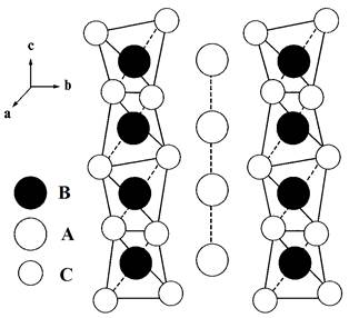
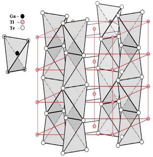
A3B3C62 compounds exhibit an hexagonal structure made of layers of A and C atoms, which form nanochains of A3,3+C6,2-2, separated by a layer of B atoms (see Figure 1). Electrical hoping-type conductivity occurs in the metallic B layer, and thus this conductivity shows a strong anisotropy.
3.1. Superionic Conductivity
Unusual properties of superionic conductors are interesting for the solving of fundamental problems of physics of condensed matter and physical chemistry, and applications [6]. An important feature of the superionic conductors is their anomalously high ionic conductivity, the order of magnitude of which is close to that typical of melts and concentrated solutions of strong electrolytic conductors. Consequently, superionic conductors can be considered as substances with hybrid properties: the conductivity of a liquid melt or solution and the mechanical strength of a solid. Crystals with structural disorders hereinafter referred to as superionic crystals, can be found in two radically different phases: at temperatures below a critical temperature, they behave similarly to ordinary ionic crystals; at temperatures above a critical temperature, they transfer to a special, superionic state. The TlGaTe2 semiconductor compound crystallizes in the tetragonal space group and features a one-dimensional (1D) rodlike structure. The electrical properties of the TlGaTe2 compound were studied in [7, 8]. The calculations of the energy band structure of TlGaTe2 showed that the top of the valence band is located at the high symmetry point T at the surface of the Brillouin zone, while the bottom of the conduction band is located at the line D [9]. The band gap obtained from performed calculations was found to be equal to 0.86 eV.
In [10, 11] it is reported about the second-order phase transition at a temperature of 98.5K. Hanias and Anagnostopoulos [12], studying the current–voltage (I–V) characteristics of a TlGaTe2 crystal, detected the effect of negative differential resistance and voltage oscillations in the region of negative differential resistance. Our investigations [4, 5, 13-20] revealed that TlGaTe2 chain crystals are subjected to phase transition in superion state, and demonstrated giant dielectric relaxation, substantial increase of dielectric permeability, and negative differential conductivity. All of these effects are connected with the transition of systems in superion state, when there is softening of Tl1+ sublattice (Figure 1), while prolonged along tetragonal axis c of crystal Ga3+-Te2-2 chains are the core of system. Univalent ions of thallium Tl1+ are reason for the intensive relaxation processes observed in system. As opposed to "classic" superion compounds, chain crystals are characterized by non-dispersion of optical and acoustic modes [1]. In super ion state the translation is broken only in one direction; so, the system passes to the superstructure state with the origin of incommensurable phases.
Within our resent studies, we investigated the dielectric and electrical properties of TlGaTe2 and TlInTe2 at temperatures above 300 K. We selected these compounds with the expectation that the crystalline structure these compounds could be considered as promising materials with superionic conductivity. The presence of a pseudogap in the density of states and the existence of ultimately anisotropic (1D) and rodlike structure in the crystals of this class makes it possible to expect specific features in electrical conductivity; these features are related to the low-dimensional type of the structure. We also studied the specific features of anisotropy of the electrical conductivity of TlGaTe2 and TlInTe2 crystals (both in the linear and nonlinear regions of the I–V characteristics) and relation of this anisotropy to both the structural features of the crystal and radiation defects. We intended to analyze the conductivity of the crystal in terms of the Mott and Pool–Frenkel models [21, 22].
To measure temperature dependences of permittivity and electrical conductivity of the crystals, we fabricated capacitors with plates of the materials under study, which served as a dielectric. Capacitor plates were made by deposition of silver conducting paste on the plate's surface. Permittivity and electrical conductivity were investigated with an E7-20 digital immitance-meter (Web-1) at a frequency of 1 MHz in the temperature range 100-450 K. The amplitude of a measuring field did not exceed 1 V/cm.
The samples were studied by THz time-domain spectroscopy, which can record the entire THz spectral response (0.1–3 THz) in a single measurement. Our classical setup has been modified to focus most of the THz beam onto a small sample, whose sizes are typically on the order 10–20 mm2.
3.2. THz Time-domain Spectroscopy
Investigations in the far infrared region could give additional information on the physics of A3B3C62 nanofibrous crystals. Here, the samples have been first studied by THz time-domain spectroscopy, which permits recording the entire THz spectral response (0.1–3 THz) in a single measurement. Our classical setup has been modified to focus most of the THz beam onto a small sample, whose sizes are typically on the order of 10–20 mm2.
The classical THz measurements were done in collaboration with IMEP-LAHC (University of Savoy, France) in a homemade spectrometer. In classical THz time-domain spectroscopy (THz-TDS), one records the temporal waveform impinging onto and transmitted by the sample. Then a numerical Fourier transform of both signals is performed. The ratio of the transmitted fast Fourier Transform (FFT) and the incident FFT spectra gives the transmission coefficient of the sample. If the origin of time is preserved between the two requested measurements, then the FFT gives both modulus and phase of the transmission coefficient. If the sample is a slab with parallel sides, the index of refraction and the coefficient of absorption could be accurately determined using an inverse electromagnetic method. This method as well as derived ones are based on the linearization of the phase at low frequencies, and thus the knowledge of the phase at a lower frequency is necessary to determine the sample parameters at the next frequency step. In materials exhibiting a high absorption band, the transmitted signal within this band could be weaker than noise. In this case, the transmission coefficient is almost zero in modulus, and its phase is unknown. The usual solution to this problem is to perform THz-TDS in reflection. However, the disadvantage of the reflection technique is its weak precision due to difficulty in achieving an appropriate reference signal. This latter is supplied by a metallic mirror located at the position of the sample, whose coefficient of reflection is supposed to be 100 %. But even a small error in position of the mirror, for example a few microns far from the actual position of the sample, leads to dramatic errors, mostly concerning the refractive index of the sample.
Due to weak THz transmission in the absorption bands, the typical means of determining the index of refraction and coefficient of absorption are not valid. Thus, we used a method described in [4], combining measurements in both: transmission and reflection. The basic idea is to derive a rough estimation of the refractive index from reflection data, while both refractive index and absorption coefficient are also calculated from transmission data. A Kramers-Kronig calculation allows us to determine the refractive index from the absorption spectrum measured in transmission. In the spectral regions of transparency, both refractive indices determined from reflection and calculated from transmission should be superimposed. To achieve superimposition, we add the necessary missing 2mπ (where m is any integer) to the phase values just after each high absorption region. We observe several absorption peaks in the THz transmission spectrum of TlInSe2 (Figure 2).
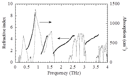
Most
of them could be attributed to the excitation of phonons (A2u and Bu)
[1, 23]. The absorption line at approximately 0.2 THz, seen only when the THz
field is aligned along the nanofibers, occurs at a frequency lower than the
lowest phonon one (A2u). Therefore, this frequency is probably
related to the libration oscillation of the ![]() nanofibers.
It is remarkable that the similar results were obtained for TlGaTe2 [5];
namely it was observed that the absorption line at approximately the same
frequency (0.2 THz), seen only when the THz field was aligned along the
nanofibers.
It is remarkable that the similar results were obtained for TlGaTe2 [5];
namely it was observed that the absorption line at approximately the same
frequency (0.2 THz), seen only when the THz field was aligned along the ![]() nanofibers.
nanofibers.
3.3. γ-irradiation Control
In [4] the conductivity in the ohmic region over the allowed band in the direction of chains and perpendicularly to them is accomplished by thermally excited charge carriers in TlGaTe2 single crystals as temperature is lowered in the range 300–90 K. As temperature is lowered, the charge transport is accomplished by hops of charge carriers over localized states near the Fermi level; these hops are more energetically favourable although they are more distant spatially. As temperature is lowered further, the conventional hopping conductivity is observed, in which case the mean length of a hop for charge carriers amounts to a value on the order of the mean distance between impurities and does not change as temperature varies.
After preliminary measurements of the values of σ|| (T) and σ⊥ (T), the samples were subjected to irradiation with γ-ray photons from a standard Co60 source. The radiation dose was increased gradually for each of studied samples by sequential exposures to the γ-ray radiation to the dose as high as 250 Mrad. Gamma rays passing through a crystal mainly interact with an electronic subsystem. The cross section of their interaction with atomic nuclei of a lattice is negligible in comparison with the cross section of the interaction with electrons. The interaction of gamma rays with the electronic subsystem is observed in the form of three main processes: photoeffect, Compton's effect, and formation of electron-positron couples. The impact of Со60 γ-irradiation with energy of 1.17 and 1.33 Mev (in our experiments this energy of γ-irradiation was used) mainly causes the creation of Compton electrons, whereas the cross section of photoabsorption is less than a percent of the cross section of Compton dispersion; and the formation of electron-positron couples is negligible at these energies.
The dose rate of γ-irradiation was 60 rad/sec. Consequently, the period of radiation varied in the interval of 20-50 days for the doses 100-250 Mrad. Heating of the samples during the irradiating was not observed. As temperature is lowered to the value at which thermal activation of charge carriers to the conduction band sets in, the dependence σ(T) becomes linear, which is the characteristic of the band conductivity. Experimental results show that, after the γ-irradiation, impurity energy levels caused by radiation defects appear in the band gap. Thermal occupation of these levels occurs at temperatures lower than that of unirradiated crystal; i.e., the temperature range of existence of thermally activated conductivity is widened. For this temperature range, it is also characteristic that, in this range, temperature related occupation of the trap centres occurs; as a result, the localized charged impurities become neutral.
4. Theoretical Model
Earlier, we used the Mott approximation to calculate the values of the density of localized states Nf, the activation energy Ea, the hop lengths R, the difference between the energy states ΔE in the vicinity of the Fermi level, and the concentrations of deep traps Nt at various doses of γ-irradiation for TlGaTe2 crystals [5]. The analysis of the dependence σ ∝ E1/2 with the thermofield Pool–Frenkel effect taken into account shows that the current in the nonlinear portion is caused by a small-magnitude field effect in the course of measurements in the case of parallel and perpendicular directions with respect to the tetragonal crystallographic axis of TlGaTe2.
We also determined the values of the concentration of ionized centres Nf, the free-path length λ, the Frenkel coefficients β, and the shape of the potential well in unirradiated TlGaTe2 crystals and the crystals irradiated with a dose of 250 Mrad. TlInTe2 crystals were studied in similar manner. The temperature dependences of electrical conductivity σ|| (T) and σ>⊥(T) of initial TlInTe2 samples (curves 1) and the samples subjected to γ-ray irradiation (curves 2–5) are shown in Figs. 3 and 4.
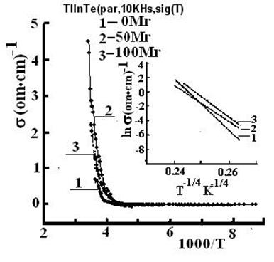
As the radiation dose is increased to 100 Mrad, the conductivity decreases and remains constant in the dose range of 100–200 Mrad; further increase in the radiation dose brings about an increase in the conductivity. Charged defects appearing as a result of irradiation with γ-ray photons play the dominant role in these processes. The conductivity can be evaluated if we take into account that the doses higher than 150–200 Mrad for these crystals apparently represent only slight ionizing radiation and acts as an activating factor for such processes as: migration of defects caused by interchain disorder and transition of metastable states to stable states; i.e., radiation-stimulated healing of structural defects is observed and leads to an increase in the electrical conductivity of the crystal.
In Table 1, we list the calculated values of the concentration of ionized centres Nf and free path lengths λ of charge carriers; the calculations were performed in the context of the Pool–Frenkel approximation [21]. As can be seen from the table, irradiation of samples leads to pronounced anisotropy of the parameters.
The
anisotropy of the free-path lengths λ of charge carriers is ![]() before irradiation and is
before irradiation and is ![]() after irradiation with a dose of 250
Mrad. The irradiation-induced increase of the free-path lengths parallel and
perpendicular to the chains is
after irradiation with a dose of 250
Mrad. The irradiation-induced increase of the free-path lengths parallel and
perpendicular to the chains is ![]() and
and ![]() respectively. The corresponding
ratios for concentrations of ionized centres are equal to
respectively. The corresponding
ratios for concentrations of ionized centres are equal to ![]() and
and ![]() ,
respectively. Thus, we may state that irradiation with a dose of 250 Mrad
causes the change of parameters of electronic subsystem.
,
respectively. Thus, we may state that irradiation with a dose of 250 Mrad
causes the change of parameters of electronic subsystem.
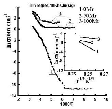
Table 1. Conductivity parameters calculated using the Pool–Frenkel approximation.
|
Direction of Conductivity |
l, cm |
Nf, cm-3 |
|
s||, initial sample |
10.4 × 10⁻⁷ |
13.7 × 10¹⁶ |
|
s^, initial sample |
9.8 × 10⁻⁶ |
1.8 × 10³ |
|
s||, irradiated with the dose 250 Mrad |
1.6 × 10⁻⁴ |
9.3 × 10¹⁷ |
|
s^, irradiated with the dose 250 Mrad |
4.3 × 10⁻⁴ |
1.1 × 10¹⁰ |
5. Application Perspective
There are many articles devoted to the investigation of superion state and possibility of creation of electrolytic accumulators based on superion materials; memory cells, capacitors with large capacity based on nanomaterials and mesoscopic structures, and low cost varistors. Superion conductors are a special class of materials given much attention. The unusual and paradoxical properties of these materials make them interesting objects for studying the fundamental problems of solid state physics as well as for prospective real-world application.
5. 1. Varistors with Controlled Parameters
It is noteworthy that the described effect of the field-induced stepwise disordering makes possible to implement the superionic state of A3B3C62 crystals under convenient conditions, which offers interesting opportunities for its application as varistors. The detailed analysis of varistor effect in semiconductors is given in [5, 24].
As stated above, irradiation with a dose of 250 Mrad causes re-ordering of nanochains (nanoneedles) and, as a consequence, an increase in the free-path length of charge carriers, which is observed in the nonlinear region of the I–V characteristic. In our opinion, the potential re-ordering the nanochains in these crystals under γ-ray irradiation offers new prospects in the design of nano-size varistors with controlled parameters.
5.2. Solid Electrolytic Accumulators
arried out experiments showed that the TlGaTe2 compound and its structural analogs: TlInSe2, TlInTe2, TlSe (Tl+1Tl+3Se2), TlS (Tl+1Tl+3S2) and TlTe (Tl+1Tl+3Тe2) compounds are subjected to phase transitions in superion state. Due to the nanofibrous (nanochain) structure of crystals of this family, the disorder of Tl+ sublattice occurs, while, nanodimensial chains of In+3Se2-2 - TlInSe2, In+3Тe2-2 - TlInTe2, Tl+3Se2-2 - TlSe and Tl+3S2-2 - TlS make up topologically disordered mesoscopic structures (Figure 5). Such mesoscopic systems possess a number of unique properties, which are not observed in usual 3D structures, namely: giant dielectric permeability [25], giant magnetic reluctances, Fogel-Fulcher's law implementation, giant dielectric relaxation, terahertz libration oscillations and other peculiarities. The peculiarities of the crystals of the TlGaTe2 family in superion phase, namely, existence of nanofibrous topologically disordered structure, allows to construct electrolytic accumulators with parameters exceed in quality than known samples [26].
5.3. Capacitors
In nanoelectronics, due to toughening technological regulations and the reduction of power supply (< 0.5 V), the necessity of using micron scale high capacity capacitors has drastically increased. Traditional capacitors do not have necessary density of capacity, radiation, and temperature hardness. The analysis of literature data [26-34] shows that development of nanoion supercapacitors based on new superion conductors is necessary.
Expert analysis of corporation growth in the industry of passive electron components marks out supercapacitors as promising group of devices. Analyzing the global market, the experts conclude that due to the use of nanotechnology the technical characteristics of supercapacitors are rapidly improved, and the cost per farad and stored energy is steadily decreased. Since 1990s supercapacitors have been widely used in electronics; more and more are needed to autonomous sources with high energy density, capacityand power.
Record high capacitive and frequency characteristics can be reached by applying advanced superionic conductors (AdSIC) [26, 30-34]. In the firm ion sublattice of these compounds there are structural canals on which the are mobile ions of opposite sign. AdSIC have record high levels of ion-transport characteristics – ion conductivity σi=0.3 Om-1cm-1 (RbAg4I5), energy of activation Еj=0/1 eV, which define the concentration of mobile ions ni=Niexp(Ei/kBT). Considering the above presented analysis we conclude that A3B3C62 type semiconductors are promising materials in the development of high capacitance capacitors, due to the high capacitance in superion.
6. Conclusion
Within the presented project, we have reviewed the physical characteristics of A3B3C62 type semiconductors and analyzed the application prospects of these crystals. Due to their unique crystalline structure, these semiconductors can be used as basis materials in the development of nano-size electronic devices, including varistors, solid electrolytic accumulators, and supercapacitors.
We have shown that the conductivity mechanism of A3B3C62 type semiconductors can be affected by different doses of γ-irradiation. This phenomenon shows A3B3C62 semiconductors to be promising material in the design of electronic devices with controlled parameters.
References
[1] A.M. Panich, R.M. Sardarly "Physical properties of the low dimensional A3B3 and A3B3C62 compounds", Nova Science Publishers, New York, 2010, p. 310. View Book
[2] L.V. Keldysh "Excitons in semiconductor-dielectric nanostructures" Physica Status Solidi (a) 164, 1997, 3–12. View Article
[3] J. Salfi, I.G. Savelyev, M. Blumin, S.V. Nair, H.E. Ruda "Direct Observation of Single-charge-detection Capability of Nanowire Field-effect Transistors", Nature Nanotechnology Letters, 5, 2010, 737-741. View Article
[4] R.M. Sardarly, O.A. Samedov, A.P. Abdullayev, E.K. Huseynov, F.T. Salmanova, G.R. Safarova "Specific Features of Conductivity of γ-Irradiated TlGaTe2 Crystals with Nanochain Structure", Semiconductors, 44, 2010, 1-5. View Article
[5] R. Sardarly, O. Samedov, N. Aliyeva, R. Aqayeva, T. Musazade, A. Sardarli "Superionic Conductivity and Specific Effects Induced by γ-Radiation in Nanofibrous TlGaTe2 Crystals" International Journal of Theoretical and Applied Nanotechnology, 1(1), 2012, 21-29. View Article
[6] L.S. Parfen'eva, A.I. Shelykh, A.I. Smirnov, A.V. Prokof'ev, V. Assmus, Kh. Misiorek, Ya. Mukha, A. Jezhovski, I.G. Vasil'eva "Heat Transport over Nonmagnetic Lithium Chains in LiCuVO4, a New One-Dimensional Superionic Conductor", Physics of Solid State, 45, 2003, 2093-2098. View Article
[7] G.D. Guseynov, E.M. Ramazanzade, E.M. Kerimova, M.Z. Ismailov "About a Group of Three-Component Compounds being Analogous to Binary Semiconductors of the AIII BVI Type" , Physica Status Solidi (b), 22, 1967, K117-K122. View Article
[8] G.D. Guseinov, G.B. Abdullayev, S.M. Bidzinova, F.M. Seidov, M.Z. Ismailov, A.M. Pashayev "On new analogs of TlSe-type semiconductor compounds", Physics Letters A, 33, 1970, 421-422. View Article
[9] É.M. Godzhaev, G.S. Orudzhev, D.M. Kafarova "Band structure and permittivity of the TlGaTe2 compound", Physics of Solid State, 46, 2004, 833-835. View Article
[10] M.A. Aldzhanov, K.K. Mamedov, A.A. Abdurragimov "Heat Capacity and Moments of the Phonon Spectrum in TlGaTe2", Physica Status Solidi (b), 131, 1985, K35–K37. View Article
[11] V.A. Aliev, M.A. Aldzhanov, S.N. Aliev "Incommensurate phase transition in TlGaTe2" JEPT Letters, 45, 1987, 534-536. View Article
[12] M.P. Hanias, A.N. Anagnostopoulos "Negative-differential-resistance effects in the TlGaTe2 ternary semiconductor", Physical Review B, 47, 1993, 4261–4267. View Article
[13] A.I. Nadjafov, G.G. Guseynov, O.Z. Alekperov, R.M. Sardarly, A.P. Abdullaev, N.A. Eyubova "Electrophysical properties and polymorphic modification TlSe" Crystallography, 53, N 5, 2008, 781-785.
[14] R.M. Sardarly, N.T. Mamedov, K. Wakita, Y. Shim, O.A. Samedov, E.A. Zeynalova "Dielectric properties, conduction mechanism, and possibility of nanodomain state with quantum dot formation in impurity-doped gamma-irradiated incommensurate TIInS2" Physica Status Solidi 2006(a) 203, No.11, 2006, 2845-2851. View Article
[15] R.M. Sardarly, O.A. Samedov, A.I. Nadzhafov, G.P. Safarova, A.A. Bayramov, F.T. Salmanov "Study of anisotropy of electrical properties intercalated TlInS2 Ge relaxors" VI International Conference on Inorganic Materials, 2008, Drezden, Germany, #35. View Article
[16] R.M. Sardarly, O.A. Samedov, A.I. Nadzhafov, F.T. Salmanov, A.P. Abdullaev, A.A. Bayramov "Relaxor Properties and Conduction in TlInS2 Crystals" Proceedings of 2nd Integration and Commercialization of Micro and Nanosystems International Conference & Exhibition, Kowloon, Hong Kong, 2008, #MNC2008-70349, p.371-375. View Article
[17] R.M. Sardarly, O.A. Samedov, A.P. Abdullaev, G.P. Safarova, A.A. Bayramov, F.T. Salmanov "The features of electroconductivity of γ-irradiated TlGaTe2 monocrystals" Abstracts Book V Erasian Conference "Nuclear science and its application", Ankara 2008, Turkey. View Article
[18] R.M. Sardarly, O.A. Samedov, A.P. Abdullaev, G.P. Safarova, A.A. Bayramov, F.T. Salmanov "Features of conductivity anisotropy of intercalated nanodimentional relaxor TlInS2
[19] R.M. Sardarly, O.A. Samedov, A.P. Abdullaev, A.I. Nadjafov, F.T. Salmanov "FTT-2009, The actual problems of a solid state physics" Proceedings, Minsk - 2009, 3, 32-34. View Article
[20] R.M. Sardarly, O.A. Samedov, A.P. Abdullayev, A.A. Bayramov, F.T. Salmanov "About Terahertz Generation on the Superstructures Layers A3B3C62 Crystals" Proceedings of IMECE'2009 ASME International Mechanical Engineering Congress and Exposition, Florida, USA. View Article
[21] Ya.I. Frenkel "Collection of Selected Works", Nauka, Moscow, 2, 1958, 217 [in Russian]. View E-Book
[22] N.F. Mott and E.A. Davis "Electronic Processes in Non-Crystalline Materials", Clarendon, Oxford, 1979, p. 604. View Article
[23] N.M. Gasanly, A.F. Goncharov, B.M. Dzhavadov, N.N. Melnik, V.I. Tagirov, E.A. Vinogradov "Vibrational Spectra of TlGaTe2, TlInTe2, and TlInSe2 Layer Single Crystals" Physica Status Solidi B 97, 1980, 367-377. View Article
[24] A.N. Pavlov, I.P. Raevskii "Varistor effect in semiconductor ferroelectrics" Technical Physics, 42, 1997, 1390-1394. View Article
[25] R. Sardarly, O. Samedov, A. Abdullayev, F. Salmanov, A. Urbanovic, F. Garet, J.-L. Coutaz "Superionic Conductivity in One-Dimensional Nanofibrous TlGaTe2 Crystals" Japanese Journal of Applied Physics, 50, 2011, 05FC09-1-05FC09-1. View Article
[26] S. Yamaguchi "Nanoionics - Present and future prospects" Science and Technology of Advanced Materials, 8, 2007, 503. View Article
[27] А. Despotuli, А. Andreeva "Nanoion devices in deep subvoltage nanoelectronics" Nanoindustry, 2008, No 5(11), 12-16. View Article
[28] А. Despotuli, А. Andreeva, V. Rambaby "Nanoionics-basis of creation new devices for MST" Nano- and Microsystem technics, V, N2, 2005, 5. View Article
[29] A.L. Despotuli, V.I. Nikolaichic "A step towards nanoionics" Solid State Ionics 60, 1993, 275–278. View Article
[30] R.K. Cavin, V.V. Zhirnov "Generic device abstractions for information processing technologies" Solid-State electronics 50, 2006, 520–526.View Article
[31] G.F. Cerofolini "Realistic limits to computation I. Physical limits" Journal of Applied Physics A 86, 2007, 23–29. View Article
[32] J. Maier "Nanoionics: ion transport and electrochemical storage in confined systems" Nature Materials 4, 2005, 805–815. View Article
[33] R. Waser, M. Aono "Nanoionics-based resistive switching memories" Nature Materials, 6, 2007, 833–840. View Article
[34] J. Garcia-Barriocanal, A. Rivera-Calzada, M. Varela, Z. Sefrioui, E. Iborra, C. Leon, S.J. Pennycook, J. Santamaria "Colossal ionic conductivity at interfaces of epitaxial ZrO2:Y2O3/SrTiO3 heterostructures" Science 321, 2008, 676–680. View Article