International Journal of Theoretical and Applied Nanotechnology (IJTAN)
ISSN: 1929-1248

Volume 1, Issue 1, Year 2012 - Pages 105-110
DOI: 10.11159/ijtan.2012.016
Negative Differential Resistance in GaN/AlN Heterostructure Nanowires
Andy Shih, Saeed Fathololoumi, Songrui Zhao, Binh Le Huy, Hieu Pham Trung Nguyen, Ishiang Shih, Zetian Mi
McGill University, Department of Electrical and Computer Engineering,
3480 University Street, Montreal, Quebec, Canada H3A 2A7
zetian.mi@mcgill.ca
Abstract - III-V semiconductor nanowire heterostructures have experienced great progress in numerous mid- and far-infrared ranges. In this work, the electrical properties of GaN/AlN nanowire heterostructures, oriented along the [0001] polar direction and grown vertically on a Si substrate by molecular beam epitaxy, were studied in the context of resonant tunneling. The negative differential resistance was observed in I-V measurements at room temperature and at 78 K for single nanowire devices, confirming the presence of resonant tunneling through AlN barriers. A peak-to-valley ratio of 1.4 was achieved. Effects of different doping profiles have been investigated, showing slight improvement of the resonant tunneling in the presence of silicon doping. This work represents a preliminary step in developing GaN nanowire based intersubband devices for far-infrared and telecom wavelength lasers and photodetectors.
Keywords: GaN, AlN, III-V Nanowire, Intersubband Transition, Resonant Tunneling, Negative Differential Resistance
© Copyright 2012 Authors - This is an Open Access article published under the Creative Commons Attribution License terms. Unrestricted use, distribution, and reproduction in any medium are permitted, provided the original work is properly cited.
1. Introduction
The transport properties of semiconductor multiple quantum well (MQW) heterostructures was first studied by Esaki and Tsu (1970). Not long after, Kazarinov and Suris suggested using the superlattice heterostructures for the amplification of electromagnetic waves via intersubband transitions (Kazarinov and Suris, 1971). Intersubband transitions in the conduction band would allow for the absorption and emission of infrared photons, which is not feasible in the interband scheme. However, the intersubband light amplification requires resonant tunneling in order to operate in the electrically stable positive differential resistance regime. Resonant tunneling occurs when two energy states from two separate quantum wells anticross across a barrier at a given electric field. Moreover, resonant tunneling can be characterized by either a coherent or sequential transport mechanism. In the former case, the large anticrossing between the coupled states results in a Fabry-Perot like carrier transport. However, in the latter case that is also known as sequential tunneling, significant electron scattering within the well makes each quantum tunneling independent of each other (Aleshkin et al., 2006). For the case of sequential tunneling (with coupling strength of Ω and dephasing time of τ//) and electron scattering (with rate of τ2-1), it was found that the transport becomes coherent if 4Ω2τ2 τ|| >> 1 and is incoherent if 4Ω2τ2 τ|| << 1 (Kazarinov and Suris, 1971).
MQWs in conjunction with intersubband transitions have led to the development of quantum cascade lasers (QCL) with emission spectra in the mid- and far-infrared (Williams, 2007). The first QCL, lasing at 4.2 μm, was demonstrated by Faist et al. (1994) at Bell Labs. Numerous applications involving QCL have emerged since the Bell Labs development such as high-resolution spectroscopy, terahertz imaging for non-invasive inspection, and plasma diagnostics (Williams, 2007; Hu, 2008). Moreover, MQW heterostructures can be utilized as functional devices such as multiple-valued memory cells (Seabaugh et al., 1992) by taking advantage of its negative differential resistance (NDR), the signature property of resonant tunnelling (Capasso and Kiehl, 1985). NDR is a property that manifests itself in the current-voltage (I-V) characteristics where the rate of change goes from positive to negative as the voltage across the device increases. This is explained through the breaking and creation of resonance between the finite states inside the quantum wells and the conduction band in the emitter side as a bias is applied (Sun, 1998). Beyond intersubband transitions and infrared emission and absorption, MQW heterostructure devices have also been designed for blue light emitting diodes (Yang et al., 2000).
During the last two decades, many groups have reported MQW structures used for intersubband emission and absorption of infrared light from III-V and II-VI materials such as GaAs/AlGaAs, InAs/AlSb, and ZnO/MgZnO (Helm et al., 1988; Warburton et al., 1995; Ohtani et al., 2009). More recently, GaN and its nitride alloys have attracted a lot of attention due to its high conduction band offset with AlN (1.7 eV) (Rigutti et al., 2010), allowing for deep confinement of states within the quantum wells, short relaxation times of less than 150 fs (Iizuka et al., 2000; Hamazaki et al., 2004), allowing for the development of high frequency oscillators and ultrafast optical switches, and large longitudinal optical (LO) phonon energy of 92 meV, allowing for photon emission in the wavelength regions that was not accessible previously (e.g. between 30 and 70μm and below 2.5 μm, as small as 1.08 μm) (Kishino et al., 2002). The GaN/AlN system can thus be designed for the fiber-optics transmission wavelength range of 1.3 to 1.55 μm (Kandaswamy, 2008).
Unfortunately, GaN-based resonant tunneling diodes still remains a challenge in terms of producing repeatable NDR with a large peak-to-valley ratio, both at cryogenic and room temperature (RT) conditions (Bayram et al., 2010). In c-plane nitride-based RTDs, the I-V characteristics tend to degrade irreversibly after the initial voltage scan. Repeatable NDR, however, has been observed in wurtzite nitrides on nonpolar (m-plane) GaN substrates (Li et al., 2012). It has been shown that a non-polar orientation should improve resonant tunneling when compared to a polar one, and that AlN barriers, compared to AlGaN ones, will result in higher peak-to-valley ratios (Carnevale et al., 2012). This absence of reproducibility has been largely attributed to the charge trapping at dislocation sites (Golka et al., 2006). Furthermore, leakage paths through dislocations may lead to relatively small peak-to-valley ratios (1.03, Li et al.), pushing the need for dislocation free nitride structures.
III-nitrides are very interesting due to their high breakdown voltage (for GaN, 3 MV/cm), high electron mobility (for GaN, 1000-2000 cm2 V-1 s-1) and high heat capacity and thermal conductivity (for GaN, >1.5 Wcm-1K-1) (Eastman and Mishra, 2002). Unfortunately, the growth of high quality GaN/AlN heterostructures is limited due to the existing lattice mismatch (~ 2.5%) and the lack of suitable large area substrates. In this work, by virtue of strain relaxation in nanowires, we have grown high quality GaN/AlN 1D heterostructures with very low threading dislocation density (Wang et al., 2012; Nguyen et al., 2011; Fathololoumi et al., 2011; Rigutti et al., 2010). The free lateral surfaces of the nanowire allow for strain relaxation, preventing dislocations from appearing within the nanowire structure (Glas, 2006). Here, we report the negative differential resistance in GaN/AlN multiple quantum well heterostructure nanowires.
2. Fabrication and Results
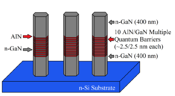
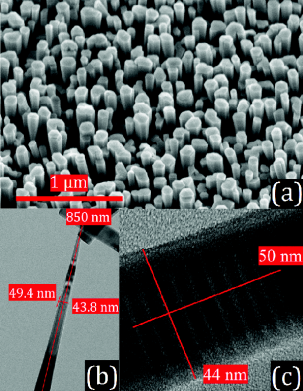
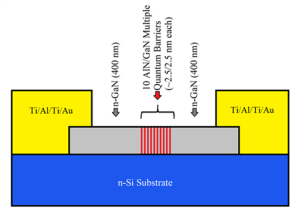
The GaN/AlN heterostructure nanowires with 10 AlN barriers were grown on Si (111) substrates using self-catalytic growth process, by radio-frequency plasma-assisted molecular beam epitaxy. The growth process was performed under nitrogen rich conditions, favouring the formation of the nanowire structure as opposed to a planar one. Furthermore, a self-catalytic growth process involving Ga droplets on the surface of the silicon substrate is preferred to avoid any unwanted contamination with metal catalysts that are typically used in other III-V nanowire growth procedures (Calarco et al., 2007). The nanowires are oriented along the [0001] polar direction with their sidewalls being non-polar m-planes. The diagram of the nanowire structure can be seen in Fig. 1-a. High-resolution scanning electron microscopy, shown in Fig. 2-a, depicts dense hexagonal nanowires, uniformly distributed across the wafer. A closer look at the transmission electron micrograph of the nanowires reveals that the structures are grown nearly free of dislocations (see Figs. 2-b-c). Moreover, micro-photoluminescence measurements were performed (shown in Fig. 3) with a HeCd laser (λ ~ 325 nm), a high-resolution spectrometer and a photomultiplier tube. A strong peak is observed at 3.42 eV with a narrow FWHM of 0.1 eV, indicating nanowires of high quality. In addition, there is no sign of yellow luminescence at ~2.2 eV at RT in the μ-PL measurements. Yellow luminescence in GaN is said to arise from transitions between the conduction band (or shallow donors) and deep acceptor levels (Shalish et al., 1999). This phenomenon can severely degrade the performance of optoelectronic devices by creating a secondary recombination path (Kucheyev et al., 2002). The nanowires have a height of ~850 nm and a diameter of ~45 nm near the GaN/AlN periodic structure. Tapering and consequently coalescence of the GaN/AlN nanowires also appear to occur, as shown in Figs. 2-a-b. In our case, tapering is partly caused by the introduction of the AlN disks. The slower migration rate of Al atoms versus Ga atoms leads to a slower vertical growth rate of AlN compared to GaN and ultimately wider diameters at the AlN disks. Coalescence of the nanowires can lead to unwanted electrical behaviour with current bypassing the periodic tunnelling structure and effectively shorting the device. Tapering of the nanowires can possibly be controlled by a Ga-flux during the growth process (Meijers et al., 2006).
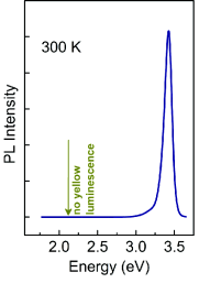
Fig. 2-c shows that ~2.5 nm thick GaN disks are separated using ten ~2.5 nm thick AlN disks, forming a multiple barrier tunneling structure. The entire AlN/GaN disks are sandwiched between two highly Si-doped (carrier concentration of ~1E19 cm-3) GaN cladding regions (length of ~ 400 nm) used to facilitate the single nanowire contact process. Three samples, denoted samples A, B, and C, with Si-doping level of ~ 0, 2E16 cm-3, and 1E17 cm-3, respectively, are utilized to study the effect of doping on the tunneling through AlN barriers. Here, we have focused on single nanowire devices to test I-V characteristics of the GaN/AlN multiple barrier tunnel junction.
The single nanowire devices were fabricated by dispersing nanowires horizontally onto a SiO2 template and by drawing the contacts using electron beam lithography to deposit metal contacts of Ti/Al/Ti/Au (10/50/10/50 nm). The single nanowire devices, shown in Figs. 4 and 5, were fabricated using the three different Si-doped samples. I-V measurements were performed in a cryogenic test chamber at RT and at 78 K, under high vacuum (~1E-7 torr) and dark conditions. A 2400 Keithley was used to measure the I-V characteristics.
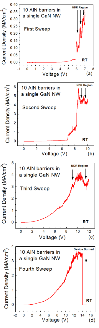
Single nanowire devices were tested with successive voltage sweeps (typically increasing in amplitude, up to 12 V). NDR was clearly observed in the nanowire, as seen in Fig. 6. However, the shape and position of the NDR peaks vary significantly between each voltage measurement. The device stability also degrades with the NDR disappearing after multiple sweeps, suggesting that dislocations and charge trapping are still present in the nanowire structure. Nonetheless, NDR was present initially in both the RT and 78 K measurements with a peak-to-valley ratio of ~1.4.
Temperature dependence tests were also performed at 78, 100, 150, 200, 250 and 300 K. In general, a clearer NDR effect was observed at lower temperatures. In devices that displayed little NDR at RT but prominent NDR at low temperatures, lower resistivity at lower temperatures was also observed. Similar results were achieved for AlGaAs/GaAs superlattice structures as previously shown (Capasso et al., 1985). However, Rigutti observed the opposite in which decreasing the temperature leads to higher resistivity and more prominent NDR in GaN/AlN superlattice nanowires (Rigutti et al., 2010). In our case, there is the possibility of a "hard breaking" in the device, in which a permanent physical change has occurred due to electrical stress. Hysteresis was also observed in the nanowires displaying NDR when the voltage was swept back towards zero, and can be attributed to the bias-dependent trapping of electrons in the quantum wells (Belyaev et al., 2003).
Ensemble nanowire samples were also tested. In general, no noticeable NDR was present in the RT experiments, due to non-uniformity of the nanowires over the large area. However, the NDR was found when testing ensemble nanowire devices at 78 K. The ensemble nanowire samples achieved a peak-to-valley ratio of ~1.2. Moreover, it was found that doping the nanowires with Si improved slightly the occurrence of NDR in the I-V characteristics for both the single nanowire and ensemble nanowire devices.
3. Conclusion
In conclusion, GaN/AlN multiple quantum well nanowires have been grown by radio-frequency assisted molecular beam epitaxy. Although negative differential resistance was only observed at 78 K for the ensemble nanowire samples, it was found to be present at 78 K as well as room temperature for the single nanowire devices, an important step forward in achieving room temperature infrared emission and absorption via intersubband transitions. A peak-to-valley ratio of ~1.4 was found; however, repeatability of the I-V measurements still remains an issue. Moreover, the effects of Si doping did appear to improve slightly the negative differential resistance. Future works will involve more in depth characterization of doping and annealing effects on the electrical performance of the nanowires. Variations in the well and barrier widths will be optimized to achieve higher transmission coefficients (shorter tunneling time).
Acknowledgements
The authors would like to acknowledge the financial support from the Natural Science and Engineering Research Council of Canada (NSERC), the Fonds de recherche du Qué ébec (FQRNT), as well as the Canadian Foundation for Innovation (CFI).
References
Aleshkin, V. Y., Reggiani, L., Rosini, M. (2006). Comparative analysis of sequential and coherent tunneling models in resonant diodes. Physical Review B, 73, 165320-1 - 165320-9. View Article
Bayram, C., Vashaei, Z., Razeghi, M. (2010). Reliability in room-temperature negative differential resistance characteristics of low-aluminum content AlGaN/GaN double-barrier resonant tunneling diodes. Applied Physics Letter, 97, 181109. View Article
Belyaev, A. E., Foxon, C. T., Novikov, S. V., Makarovsky, O., Eaves, L. (2003) Comment on "AlN/GaN double-barrier resonant tunneling diodes grown by rf-plasma-assisted molecular-beam epitaxy" [Applied Physics Letter 81, 1729 (2002)]. Applied Physics Letter, 83, 17, 3626-3627. View Article
Calarco, R., Meijers, R. J., Debnath, R. T., Stoica, T., Sutter, E., Lüth, H. (2007). Nucleation and Growth of GaN Nanowires on Si(111) Performed by Molecular Beam Epitaxy. Nano Letter, 7, 8, 2248-2251. View Article
Capasso, F., Kiehl, R. A. (1985). Resonant tunneling transistor with quantum well base and high-energy injection: A new negative differential resistance device. Journal of Applied Physics 58, 1366-1368. View Article
Carnevale, S. D., Marginean, C., Philips, P. J., Kent, T. F., SSawrar, A. T. M. G., Mills, M. J., Myers, R. C. (2012). Coaxial nanowire resonant tunneling diodes from non-polar AlN/GaN on silicon. Applied Physics Letter, 100, 142115. View Article
Davydov, A. V., Motayed, A., Boettinger, W. J., Gates, R. S., Xue, Q. Z, Lee, H. C., Yoo, Y. K. (2005). Combinatorial optimization of Ti/Al/Ti/Au ohmic contacts to n-GaN. Physics of the Solid State 2, 7, 2551-2554. View Article
Eastman, L. F., Mishra, U. K. (2002). The Toughest Transistor Yet. IEEE Spectrum, 39, 5, 28-33. View Article
Esaki, L., Tsu, R. (1970). Superlattice and Negative Differential Conductivity in Semiconductors. IBM Journal of Research and Development, 14, 61-65. View Article
Faist, J., Capasso, F., Sivco, D. L., Sirtori, C., Hutchinson, A. L., Cho, A. Y. (1994). Quantum Cascade Laser. Science, 264, 5158, 553-556. View Article
Fathololoumi, S., Nguyen, H. P. T., Mi, Z. (2011). Self-Organized In(Ga)N Nanowire Heterostructures and Optoelectronic Device Applications. Nanosci. And Nanotech. Asia, 2, 123-139.
Glas, F. (2006). Critical dimensions for the plastic relaxation of strained axial heterostructures in free-standing nanowires. Physical Review B, 74, 121302-1-4. View Article
Golka, S., Pflugl, C., Schrenk, W., Strasser, G., Skierbiszewski, C., Siekacz, M., Grzegory, I., Porowski, S. (2006). Negative differential resistance in dislocation-free GaN/AlGaN double-barrier diodes grown on bulk GaN. Applied Physics Letter, 88, 172106-1-4. View Article
Hamazaki, J., Matsui, S., Kunugita, H., Ema, K., Kanazawa, H., Tachibana, T., Kikuchi, A., Kishino, K. (2004). Ultrafast intersubband relaxation and nonlinear susceptibility at 1.55 μm in GaN/AlN multiple-quantum wells. Applied Physics Letter, 84, 1102-1104. View Article
Helm, M., Colas, E., England, P., DeRosa, F., Allen, S. J. Jr. (1988). Observation of grating-induced intersubband emission from GaAs/AlGaAs superlattices. Applied Physics Letter 53, 1714-1716. View Article
Helm, M., England P., Colas E., DeRosa F., Allen, S. J. Jr. (1989). Intersubband Emission from Semiconductor Superlattices Excited by Sequential Resonant Tunneling. Physical Review Letter, 63, 74-77. View Article
Hu, Q. (2008). Terahertz Quantum Cascade Lasers and Real-time T-rays Imaging at video rate. Terahertz Science and Technology. 1, 1, 1-10.View Article
Iizuka, N., Kaneko, K., Suzuki, N., Asano, T., Noda, S. (2000). Ultrafast intersubband relaxation (150 fs) in AlGaN/GaN multiple quantum wells. Applied Physics Letter, 77, 5, 648-650. View Article
Kandaswamy, P. K., Guillot, F., Bellet-Amalric, E., Monroy, E., Nevou, L., Techernycheva, M., Michon, A., Julien, F. H., Baumann, E., Giorgetta, F. R., Hofstetter, D., Remmele, T., Albrecht, M., Birner, S., Dang, L. S. (2008). GaN/AlN short-period superlattices for intersubband optoelectronics: A systematic study of their epitaxial growth, design, and performance. Journal of Applied Physics 104, 093501-1-16. View Article
Kazarinov, R. F., Suris, R. A. (1971). Possibility of amplification of electromagnetic waves in a semiconductor with a superlattice. Sov. Phys. Semicond., 5, 707.
Kishino, K., Kikuchi, A., Kanazawa, H., Tachibana, T. (2002). Intersubband transition in (GaN)m/(AlN)n superlattices in the wavelength range from 1.08 to 1.61 μm. Applied Physics Letter, 81, 7, 1234-1236. View Article
Kucheyev, S. O., Toth, M., Phillips, M. R., Williams, J. S., Jagadish, C., Li, G. (2002). Chemical origin of the yellow luminescence in GaN. Journal of Applied Physics 91, 9, 5867-5874. View Article
Li, D., Tang, L., Edmunds, C., Shao, J., Gardner, G. (2012). Repeatable low-temperature negative-differential resistance from Al0.18Ga0.82N/GaN resonant tunneling diodes grown by molecular-beam epitaxy on free-standing GaN substrates. Applied Physics Letter, 100, 252105. View Article
Meijers, R., Richter, T., Calarco, R., Stoica, T., Bochem, H.-P., Marso, M., Lüth, H. (2006). GaN-nanowhiskers: MBE-growth conditions and optical properties. Journal of Crystal Growth, 289, 381-386. View Article
Nguyen, H. P. T., Zhang, S., Cui, K., Han, X., Fathololoumi, S., Couillard, M., Botton, G. A., Mi, Z. (2011). p-Type Modulation Doped InGaN/GaN Dot-in-a-Wire White-Light-Emitting Diodes Monolithically Grown on Si(111). Nano Letter, 11, 1919-1924. View Article
Ohtani, K., Belmoubarik, M., Ohno, H. (2009). Intersubband optical transitions in ZnO-based quantum wells grown by plasma-assisted molecular beam epitaxy. Journal of Crystal Growth, 311, 2176-2178. View Article
Rigutti, L., Jacopin G., Bugallo A. D. L., Tchernycheva M., Warde E., Julien F. H., Songmuang R., Galopin E., Largeau L., Harmand J.-C. (2010). Investigation of the electronic transport in GaN nanowires containing GaN/AlN quantum discs. Nanotechnology, Vol. 21, 425206-1 - 425206-6. View Article
Seabaugh, A. C., Kao, Y.-C., Yuan, H.-T. (1992). Nine-State Resonant Tunneling Diode Memory. IEEE Electron Device Letter, 13, 9, 479-481. View Article
Shalish, I., Kronik, L., Segal, G., Rosenwaks, Y., Shapira, Y. (1999). Yellow luminescence and related deep levels in unintentionally doped GaN films. Physical Review B., 59, 15, 9748-9751. View Article
Sun, J. P., Haddad, G. I., Mazumder, P., Schulman, J. N. (1998). Resonant Tunneling Diodes: Models and Applications. Proceedings of the IEEE, 86, 4, 641-661. View Article
Wang, Q., Nguyen, H. P. T., Cui, K., Mi, Z. (2012). High efficiency ultraviolet emission from AlxGa1-xN core-shell nanowire heterostructures grown on Si (111) by molecular beam epitaxy. Applied Physics Letter, 101, 0.43115-1-4. View Article
Warburton, R. J., Gauer, C., Wixforth, A., Kotthaus, J. P. (1995). Intersubband resonances in InAs/AlSb quantum wells: Selection rules, matrix elements, and the depolarization field. Physical Review B., 53, 12, 7903-7910. View Article
Williams, B. S. (2007). Terahertz quantum-cascade lasers. Nature Photonics, 1, 517-525. View Article